-

- News
- Books
Featured Books
- smt007 Magazine
Latest Issues
Current Issue
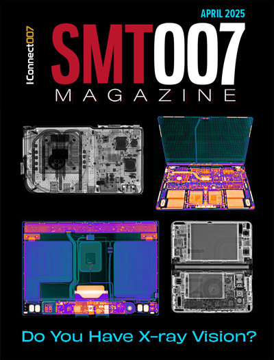
Do You Have X-ray Vision?
Has X-ray’s time finally come in electronics manufacturing? Join us in this issue of SMT007 Magazine, where we answer this question and others to bring more efficiency to your bottom line.

IPC APEX EXPO 2025: A Preview
It’s that time again. If you’re going to Anaheim for IPC APEX EXPO 2025, we’ll see you there. In the meantime, consider this issue of SMT007 Magazine to be your golden ticket to planning the show.

Technical Resources
Key industry organizations–all with knowledge sharing as a part of their mission–share their technical repositories in this issue of SMT007 Magazine. Where can you find information critical to your work? Odds are, right here.
- Articles
- Columns
Search Console
- Links
- Media kit
||| MENU - smt007 Magazine
Book Excerpt: The Printed Circuit Designer’s Guide to... DFM Essentials, Ch. 1
October 25, 2024 | I-Connect007Estimated reading time: 1 minute
Excerpt from: The Printed Circuit Designer’s Guide to... DFM Essentials
By Anaya Vardya, American Standard Circuits / ASC Sunstone Circuits
Chapter 1: Materials
Standard Multilayer Materials
Most PCBs are manufactured using three basic materials: glass-reinforced epoxy laminate, prepreg, and copper foil. PCBs are constructed from three basic material types: copper foil, prepreg, and cores.
Copper foil: Sheets of copper foil are incorporated into the outer layer of the PCB, laminating it onto the prepreg to create the outer layers. Outer layers are generally constructed using ½-ounce copper or thicker depending on the design requirements. Internal layers are constructed with copper that is specified on the fabrication print. Half-ounce copper foil is commonly used for signal layers; 1 ounce for plane layers, and 2 ounce or greater for power planes where there is a high DC current. Other thicknesses may be used based on the design requirements.
Prepreg: This is a semi-cured glass resin material. The resin used for the FR-4 type materials is epoxy-based. There is no copper attached to this material.
Core: This is fully cured glass-resin material with copper laminated to both sides. This is typically used for internal layers. It is occasionally used for outer layers, but that is not a preferred construction method. A core is constructed from either one sheet of prepreg (single ply) or two or more sheets of prepreg, and two layers of copper foil. Single ply is considered the preferred core construction and has better dimensional stability.
High-frequency (RF/Microwave) Materials
High-frequency designs (1 GHz and up) require materials with closely controlled dielectric constants and dissipation factors. The FR-4 materials normally used for PCBs don’t have the desired controlled characteristics. The substrate materials used for high-frequency applications were originally based upon PTFE resin formulations that have the desired properties, i.e. dielectric constant (Dk) controlled to +/- 0.04 and dissipation factor (Df) to 0.0004. These values may vary somewhat depending on the material type and supplier. Today, there are a number of materials on the market that do not contain PTFE resin but still have controlled values that can be used for high-frequency applications.
Visit the I-Connect007 library to continue reading The Printed Circuit Designer’s Guide to... DFM Essentials.
Suggested Items
Elephantech: For a Greener Tomorrow
04/16/2025 | Marcy LaRont, PCB007 MagazineNobuhiko Okamoto is the global sales and marketing manager for Elephantech Inc., a Japanese startup with a vision to make electronics more sustainable. The company is developing a metal inkjet technology that can print directly on the substrate and then give it a copper thickness by plating. In this interview, he discusses this novel technology's environmental advantages, as well as its potential benefits for the PCB manufacturing and semiconductor packaging segments.
Trouble in Your Tank: Organic Addition Agents in Electrolytic Copper Plating
04/15/2025 | Michael Carano -- Column: Trouble in Your TankThere are numerous factors at play in the science of electroplating or, as most often called, electrolytic plating. One critical element is the use of organic addition agents and their role in copper plating. The function and use of these chemical compounds will be explored in more detail.
IDTechEx Highlights Recyclable Materials for PCBs
04/10/2025 | IDTechExConventional printed circuit board (PCB) manufacturing is wasteful, harmful to the environment and energy intensive. This can be mitigated by the implementation of new recyclable materials and technologies, which have the potential to revolutionize electronics manufacturing.
Connect the Dots: Stop Killing Your Yield—The Hidden Cost of Design Oversights
04/03/2025 | Matt Stevenson -- Column: Connect the DotsI’ve been in this industry long enough to recognize red flags in PCB designs. When designers send over PCBs that look great on the computer screen but have hidden flaws, it can lead to manufacturing problems. I have seen this happen too often: manufacturing delays, yield losses, and designers asking, “Why didn’t anyone tell me sooner?” Here’s the thing: Minor design improvements can greatly impact manufacturing yield, and design oversights can lead to expensive bottlenecks. Here’s how to find the hidden flaws in a design and avoid disaster.
Real Time with... IPC APEX EXPO 2025: Tariffs and Supply Chains in U.S. Electronics Manufacturing
04/01/2025 | Real Time with...IPC APEX EXPOChris Mitchell, VP of Global Government Relations for IPC, discusses IPC's concerns about tariffs on copper and their impact on U.S. electronics manufacturing. He emphasizes the complexity of supply chains and the need for policymakers to understand their effects.


