-

- News
- Books
Featured Books
- smt007 Magazine
Latest Issues
Current Issue
Intelligent Test and Inspection
Are you ready to explore the cutting-edge advancements shaping the electronics manufacturing industry? The May 2025 issue of SMT007 Magazine is packed with insights, innovations, and expert perspectives that you won’t want to miss.

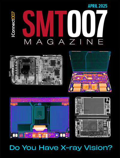
Do You Have X-ray Vision?
Has X-ray’s time finally come in electronics manufacturing? Join us in this issue of SMT007 Magazine, where we answer this question and others to bring more efficiency to your bottom line.

IPC APEX EXPO 2025: A Preview
It’s that time again. If you’re going to Anaheim for IPC APEX EXPO 2025, we’ll see you there. In the meantime, consider this issue of SMT007 Magazine to be your golden ticket to planning the show.
- Articles
- Columns
Search Console
- Links
- Media kit
||| MENU - smt007 Magazine
Estimated reading time: 5 minutes
Beyond Design: Integrated Circuit to PCB Integration
Technologies such as artificial intelligence, autonomous cars, smartphones, and wearable devices are significantly transforming the semiconductor industry. The miniaturization trend drives the IC footprint to an even smaller profile, requiring tighter margins. From the PCB designer’s perspective, smaller form factors are achievable, making devices more compact and lightweight. But double-sided SMT placement, reduced routing channels, and high-speed constraints create multiple challenges for designers. However, there are some advantages to miniaturization: shorter interconnects between the IC and the PCB reduce signal loss and electromagnetic interference. High-speed digital signals in the GHz range benefit from reduced parasitics.
Fortunately, most designers are not involved in this cutting-edge design paradigm. However, field programmable gate arrays (FPGAs) are now commonplace in most digital designs. These high-speed, high gate/pin count devices, which once only provided glue logic, are now offering embedded processors, digital signal processors (DSPs), graphics processors, memory blocks, and numerous input/output (I/O) pins in one massive ball grid array (BGA) package, not to mention the considerable number of power supplies required to power these devices. Accommodating 30 to 40 individual power supplies to the active devices is now commonplace. This added complexity has introduced many PCB layout challenges beyond the obvious fanout and route of the fine-pitch BGA.
The primary issue is generating optimal FPGA pin assignments that do not add vias and signal layers to a PCB stackup or increase the time required to integrate the FPGA with the PCB. Engineers generally do not consider FPGA pin assignments that expedite the PCB layout. Hundreds of logical signals need to be mapped to the physical pin-out of the device and harmonized with the routing requirements while maintaining the electrical integrity of the design.
To further frustrate the situation, the FPGA I/O assignment is typically in a constant state of flux throughout the design process. Consequently, many PCB designs must be reiterated simply because the board and the FPGA design teams did not have the I/O pin-out synchronized. This has happened to me in the past. The board may go through the process of pre-layout simulation, place, and route, and then a post-layout simulation to verify all the timing is perfect, only to find on testing the assembly that the FPGA I/O pin-out is incorrect on the BGA footprint. Meanwhile, after days of delays, I re-routed, ran design rule checks, re-simulated the layout, and exported the deliverables. However, delays can have financial implications.
Figure 2 shows the rather disorganized I/O connections of a first-pass FPGA pin assignment. This is typically what a PCB designer has to deal with—straight from the FPGA place-and-route tools. To make this more routable, the designer needs to adjust the pin assignment to first be on one outer edge of the BGA and then order the pins to eliminate cross-overs.
Even if we manually reassign the pin-out, the problem now is how to back-annotate this modified BGA pin assignment to the FPGA design tools. The manual process is time-consuming, tedious, and error prone. The key issue is to ensure consistency between the tool sets used in the hardware description language (HDL), FPGA, and PCB environments. We must properly represent the language-based HDL representation of the FPGA as a schematic symbol containing the correct pin data, as well as the appropriate mapping to the BGA footprint.
Alternatively, I/O optimization tools (Figure 3) can provide parallel paths of FPGA and PCB design, trimming days from the design process and delivery schedules and providing significant overall long-term cost benefits. We can meet these challenges with tools that add hardware description language (HDL) synthesis and advanced FPGA-PCB I/O optimization to the PCB layout software. This interface between the HDL design environment and the physical implementation on the PCB significantly reduces both time-to-market and manufacturing costs by automating the process, reducing errors and thus iterations.
At any stage of the project, the PCB design flow should tightly integrate I/O optimization and make it accessible. Keeping the schematic, PCB layout, and FPGA databases synchronized allows users to control the flow of design data in the project.
An FPGA vendor-neutral design environment that enables architecture-specific optimization takes advantage of the specific features of each FPGA device to meet the design requirements. Vendor-independent synthesis supports devices from Altera, Lattice, Microsemi, and Xilinx. Therefore, you can use the same HDL design source files and constraints to target any device and to obtain a synthesized netlist that can be used for place and route with the appropriate vendor tools. This vendor independence allows users to easily re-target and analyze results for any FPGA device, enabling you to find the best FPGA device to suit the design.
Automating this error-prone boundary between FPGA and PCB design makes sense. Most of the popular PCB vendors have I/O optimization tools. Cadence has its FPGA System Planner, Siemens has I/O Optimization, and Zuken has FPGA Co-design solutions. Design teams need to implement these new methodologies to ensure they do not negate the cost and time-to-market benefits of using programmable logic.
Key Points
- The miniaturization trend is driving the IC footprint to an even smaller profile, requiring tighter margins.
- Taiwan currently produces approximately 80% of the global supply of silicon chips.
- Double-sided SMT placement, reduced routing channels, and high-speed constraints are creating multiple challenges for designers.
- Shorter interconnects between the IC and the PCB reduce signal loss and electromagnetic interference.
- Accommodating 30 to 40 individual power supplies to the active devices is now commonplace. This added complexity has introduced many PCB layout challenges beyond the obvious fanout and route of the fine-pitch BGA.
- The primary issue is generating optimal FPGA pin assignments that do not add vias and signal layers to a PCB stackup, or increase the time required to integrate the FPGA with the PCB.
- Many PCB designs have to be reiterated simply because the board and the FPGA design teams did not have the I/O pin-out synchronized.
- To make a layout more routable, the designer needs to adjust the pin FPGA assignment.
- The problem is how to back-annotate this modified BGA pin assignment to the FPGA design tools.
- I/O optimization tools can provide parallel paths of FPGA and PCB design, trimming days from the design process and delivery schedules and providing significant overall long-term cost benefits.
Resources
Beyond Design: “FPGA-PCB Design Challenges” by Barry Olney
“FPGA I/O Features Help Lower Overall PCB Costs” by Dave Brady, Siemens EDA
This column originally appeared in the September 2024 issue of Design007 Magazine.
More Columns from Beyond Design
Beyond Design: Key SI Considerations for High-speed PCB DesignBeyond Design: Electro-optical Circuit Boards
Beyond Design: AI-driven Inverse Stackup Optimization
Beyond Design: High-speed Rules of Thumb
Beyond Design: Does Current Deliver the Energy in a Circuit?
Beyond Design: Termination Planning
Beyond Design: Dielectric Material Selection Guide
Beyond Design: The Art of Presenting PCB Design Courses


