


 Global Citizenship: Cultural Nuances Around the World
 The Government Circuit: Four Things to Know About IPC Advocacy in 2025


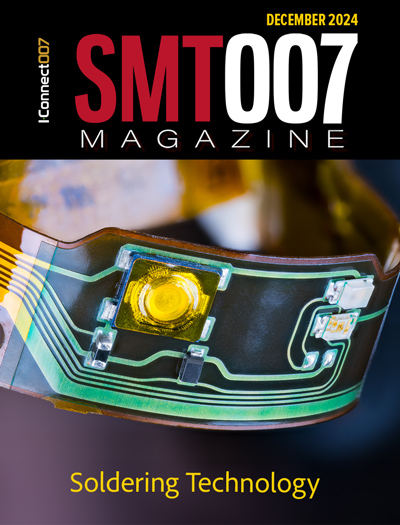
DFM 101: Final Finishes—OSP
March 9, 2023 | Anaya Vardya, American Standard CircuitsEstimated reading time: 1 minute

Introduction
One of the biggest challenges facing PCB designers is not understanding the cost drivers in the PCB manufacturing process. The next final finishes to discuss in this series is OSP. As with all surface finishes there are pros and cons with the decision of which to use. It is a combination of application, cost, and the properties of the finish. OSP is RoHS-compliant as there is zero lead content in the finish.
Final Finishes
OSP (Organic Solderability Preservative)
OSP is a thin organic coating, typically 5.9 to 11.8 µin [0.15 to 0.30 µm] thick, designed to prevent the oxidation of copper to maintain solderability over an extended period. Compared with other surface finish technologies, OSP is somewhat different. It uses a chemical process to produce an organic film on the bare copper surface which acts as a barrier to copper oxidation. OSP is organic, not metallic, and its cost is lower than most surface treatment technologies.
As with all surface finishes, the primary purpose is to protect the solderable surfaces on the PCB from oxidation and to aid in assembly soldering. This process coats a very thin coating of an organic material that inhibits copper oxidation. It is so thin that it is nearly impossible to see and measure. The organic material is removed by the assembly flux. Boards that have been OSP coated will have bright copper pad coloration. OSP is specially designed for mixed metal applications, such as electroless nickel immersion gold (ENIG). The OSP selectively deposits on copper while leaving gold connectors or metallic heat sinks free of contamination.
There are a couple of common OSP finishes widely used in the industry:
ENTEK CU-56: This is used for assemblies that will only go through a single reflow process. This finish is not being utilized much anymore because of the use of mixed technology boards (SMT and through-hole).
ENTEK CU-106A: This is the most prevalent version primarily due to the ability to survive multiple thermal assembly operations. PCBs that have multiple surface finishes can use the CU-106A(X) finish.
To read this entire article, which appeared in the February 2023 issue of Design007 Magazine, click here.
Share on:


Suggested Items
EIPC 2025 Winter Conference, Day 2: A Roadmap to Material Selection
02/20/2025 | Pete Starkey, I-Connect007The EIPC 2025 Winter Conference, Feb. 4-5, in Luxembourg City, featured keynotes and two days of conference proceedings. The keynote session and first-day conference proceedings are reported separately. Here is my review of the second day’s conference proceedings. Delegates dutifully assembled bright and early, well-rested and eager to participate in the second day’s proceedings of the EIPC Winter Conference in Luxembourg.
Designers Notebook: Addressing Future Challenges for Designers
02/06/2025 | Vern Solberg -- Column: Designer's NotebookThe printed circuit board is and will probably continue to be the base platform for most electronics. With the proliferation of new generations of high I/O, fine-pitch surface mount semiconductor package variations, circuit interconnect is an insignificant factor. Circuit board designers continually face challenges such as component quantity and complexity, limited surface area, and meeting the circuit board’s cost target. The printed circuit design engineer’s prominent position demands the development of efficiently manufacturable products that perform without compromise.
DesignCon 2025, Day 2: It’s All About AI
01/30/2025 | Marcy LaRont, I-Connect007It’s hard to get away from the topic of artificial intelligence, but why would you? It’s everywhere and in everything, and my time attending presentations about AI at DesignCon 2025 was well worth it. The conference’s agenda featured engaging presentations and discussions focused on the technological advancements in AI, big data centers, and memory innovations, emphasizing the critical relationship between processors and circuit boards.
Beyond Design: Electro-optical Circuit Boards
01/22/2025 | Barry Olney -- Column: Beyond DesignPredicting the role of PCB designers in 10 years is a challenge. If only I had a crystal ball. However, we know that as technology progresses, the limitations of copper PCBs are increasingly apparent, particularly regarding speed, bandwidth, and signal integrity. Innovations such as optical interconnects and photonic integrated circuits are setting the stage for the next generation of PCBs, delivering higher performance and efficiency. The future of PCB design will probably incorporate these new technologies to address the challenges of traditional copper-based designs.
Designers Notebook: Impact of Advanced Semiconductor Packaging on PCB Stackup
01/07/2025 | Vern Solberg -- Column: Designer's NotebookTo accommodate new generations of high I/O semiconductor packaging, printed circuit board fabrication technology has had to undergo significant changes in both the process methods and the criteria for base material selection and construction sequence (stackup). Many of the new high-function multi-core semiconductor package families require more terminals than their predecessors, requiring a significantly narrower terminal pitch. Interconnecting these very fine-pitch, high I/O semiconductors to the PCB is made possible by an intermediate element referred to as an interposer.