


 SMT Perspectives & Prospects: The Architecture of Winston Churchill’s Leadership
 Global Sourcing Spotlight: Making Global Sourcing Simple Again
 The Government Circuit: New Council Now Helps Shape Policy Decisions in the Electronics Supply Chain


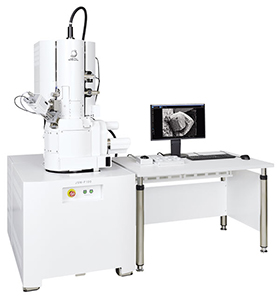
JEOL introduces a new Field Emission Scanning Electron Microscope with several features unique to the company’s FE SEM product line: NeoEngine, employing analytical intelligence for optimizing electron beam setup and tuning; embedded EDS with Live Analysis for real time imaging and elemental analysis; and Zeromag navigation function, seamlessly transitioning between optical imaging to nanoscale investigation with the high-powered optics of the SEM.
"JEOL’s F100 FE-SEM offers a truly revolutionary approach to address users’ high-resolution microscopy and microanalysis needs. In a single platform JEOL combined the best electron optics with fully embedded EDS microanalysis and the powerful AI algorithms of NeoEngine to achieve the ultimate ease of use and streamlined workflow," says Dr. Natasha Erdman, FESEM Product Manager.
NeoEngine corrects electron trajectories and automatically aligns the beam in real time, plus automatically corrects focus, brightness/contrast, and astigmatism. The SEM achieves single-digit Angstrom resolution at low kV, ideal for ultrahigh high-resolution imaging of nanostructures, specimen surface details, biological specimens, and magnetic samples as well as elemental analysis of non-conductive and beam sensitive samples.
Fully embedded EDS with Live Analysis allows the user to simply select the area, mapping, line, or another type of analysis directly on the observation screen to begin automatic live display of the elements in the specified location.
The large specimen chamber of the JSM-F100 features multiple ports for analytical applications: EDS, WDS, EBSD, STEM, BSE, and CL. An optional Soft X-ray Emission Spectrometer provides efficient and parallel collection of very low-energy X-rays while providing unprecedented chemical state analysis.
The JEOL JSM-F100 features an in-lens detector and energy filter, an Aperture Angle Control Lens (ACL) for superb resolution at any kV or probe current, Beam Deceleration (BD) mode for charge reduction and enhanced surface detail, and a variable pressure option for non-conductive specimens.
Never before has the power of Field Emission SEM been so easy to use. With the introduction of JEOL’s next-generation streamlined FE SEM product line, operator controls are simplified and the functions of the SEM fully automated for optimum performance. Imaging and analysis data are quickly obtained and reported through the effortless data management system.


