


 Global Citizenship: Redefining Connection and Responsibility in Digital Transformation
 SMT Perspectives and Prospects: Artificial Intelligence, Part 5: Brain, Mind, Intelligence
 Global Sourcing Spotlight: Watch Out! Avoiding Pitfalls in Global Sourcing


When Semiconductors Stick Together, Materials Go Quantum
March 8, 2019 | Lawrence Berkeley National LaboratoryEstimated reading time: 4 minutes
A team of researchers led by the Department of Energy’s Lawrence Berkeley National Laboratory (Berkeley Lab) has developed a simple method that could turn ordinary semiconducting materials into quantum machines—superthin devices marked by extraordinary electronic behavior.
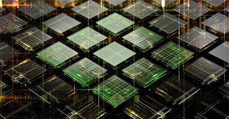
Image Caption: A method developed by a Berkeley Lab-led research team may one day turn ordinary semiconducting materials into quantum electronic devices. (Credit: iStock.com/NiPlot)
Such an advancement could help to revolutionize a number of industries aiming for energy-efficient electronic systems—and provide a platform for exotic new physics.
The study describing the method, which stacks together 2D layers of tungsten disulfide and tungsten diselenide to create an intricately patterned material, or superlattice, was published online recently in the journal Nature.
“This is an amazing discovery because we didn’t think of these semiconducting materials as strongly interacting,” said Feng Wang, a condensed matter physicist with Berkeley Lab’s Materials Sciences Division and professor of physics at UC Berkeley. “Now this work has brought these seemingly ordinary semiconductors into the quantum materials space.”
Image Caption: The twist angle formed between atomically thin layers of tungsten disulfide and tungsten diselenide acts as a “tuning knob,” transforming these semiconductors into an exotic quantum material. (Credit: Berkeley Lab) (Credit: Berkeley Lab)
Two-dimensional (2D) materials, which are just one atom thick, are like nanosized building blocks that can be stacked arbitrarily to form tiny devices. When the lattices of two 2D materials are similar and well-aligned, a repeating pattern called a moiré superlattice can form.
For the past decade, researchers have been studying ways to combine different 2D materials, often starting with graphene—a material known for its ability to efficiently conduct heat and electricity. Out of this body of work, other researchers had discovered that moiré superlattices formed with graphene exhibit exotic physics such as superconductivity when the layers are aligned at just the right angle.
The new study, led by Wang, used 2D samples of semiconducting materials—tungsten disulfide and tungsten diselenide—to show that the twist angle between layers provides a “tuning knob” to turn a 2D semiconducting system into an exotic quantum material with highly interacting electrons.
Page 1 of 2
Share on:


Suggested Items
Indium Experts to Present on Power Electronics at PCIM Europe 2025
04/17/2025 | Indium CorporationAs one of the leading materials providers to the power electronics assembly and e-Mobility industries, Indium Corporation experts will share their technical insight and knowledge on a variety of industry-related topics throughout PCIM Europe, May 6-8, in Nuremberg, Germany.
YINCAE to Showcase Cutting-Edge Solutions at SEMICON Southeast Asia 2025
04/16/2025 | YINCAEYINCAE Advanced Materials, a leading provider of innovative solutions for the semiconductor and microelectronics industries, is proud to announce its participation in SEMICON Southeast Asia 2025.
Improve Your Process Reliability: Axxon-Mycronic and HumiSeal to Host Conformal Coating Workshop in Guadalajara
04/15/2025 | Axxon-MycronicAxxon-Mycronic, a leading, global supplier of innovative and production-ready, dispensing and conformal coating systems, in collaboration with HumiSeal, a global expert in protective coating materials, is excited to announce a Conformal Coating Workshop taking place on May 8, 2025 in Guadalajara, Mexico.
Real Time with... IPC APEX EXPO 2025: Exploring LCP Materials with Matrix Electronics
04/15/2025 | Real Time with...IPC APEX EXPONolan Johnson introduces Robert Berg from Matrix Electronics, highlighting the company's focus on high-speed, low-loss flexible materials, especially LCP materials. LCP (liquid crystal polymer) is a thermal plastic with unique properties that make it ideal for advanced PCB applications. Despite processing challenges, its stability and FDA approval for medical use drive interest in aerospace and medical markets.
Dongguk University Researchers Advance Lithium-Ion Battery Technology with Hybrid Anode Material
04/14/2025 | PRNewswireResearchers from Dongguk University have achieved a significant breakthrough in lithium-ion battery technology by developing a novel hybrid anode material.