-

- News
- Books
Featured Books
- smt007 Magazine
Latest Issues
Current Issue
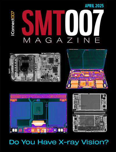
Do You Have X-ray Vision?
Has X-ray’s time finally come in electronics manufacturing? Join us in this issue of SMT007 Magazine, where we answer this question and others to bring more efficiency to your bottom line.

IPC APEX EXPO 2025: A Preview
It’s that time again. If you’re going to Anaheim for IPC APEX EXPO 2025, we’ll see you there. In the meantime, consider this issue of SMT007 Magazine to be your golden ticket to planning the show.

Technical Resources
Key industry organizations–all with knowledge sharing as a part of their mission–share their technical repositories in this issue of SMT007 Magazine. Where can you find information critical to your work? Odds are, right here.
- Articles
- Columns
Search Console
- Links
- Media kit
||| MENU - smt007 Magazine
The Vital Role of Solder Paste Printing in New Product Introduction
February 22, 2018 | Richard Barratt, JJS ManufacturingEstimated reading time: 3 minutes
Surface-mount assembly has a crucial role to play in the new product introduction (NPI) process for electronics manufacturing.
The high degree of automation within the SMT methodology offers a variety of advantages, from automatic correction of errors, to simpler and faster assembly, better mechanical performance, increased production rates and reduced labor costs.
The SMT assembly process for an electronics manufacturing services (EMS) provider can be broken down into four key stages:
- Solder paste printing
- Pick and place
- Oven profiling
- Automated optical inspection (AOI)
Depending on the complexity of the design, or your own outsourcing strategy, your product could pass through each of these processes in turn, or you may find that you omit a step or two.
In this first in a series of articles exploring SMT assembly, we highlight the specific attributes, and the vital importance, of the solder paste printing process for your NPI.
Working to Your Specifications
The first step for your EMS provider will be to analyze the PCB data that is specific to your order, to ensure that they select the required stencil thickness and the most suitable material.
Solder paste printing is the most common method of applying solder paste to a PCB. Accurate solder paste application is hugely important in avoiding assembly defects which can have a knock-on effect further down the production process. So, it is vital that this key stage is correctly managed and controlled by your EMS partner.
Solder paste is essentially powdered solder which has been suspended in a thick medium called flux. The flux acts as a kind of temporary adhesive, holding the components in place until the soldering process begins. Solder paste is applied to the PCB using a stencil (generally stainless steel, but occasionally nickel,) then once the solder is melted it forms an electrical/mechanical connection.
The thickness of the stencil is what determines the volume of solder applied. For some projects it may even be necessary to have several thicknesses in different areas within the one stencil (often referred to as a multi-level stencil).
Another key factor to consider in the solder printing process is paste release. The correct type of solder paste should be selected based upon the size of the apertures (or holes) within the stencil. If the apertures are very small, for example, then the solder paste may be more prone to sticking to the stencil and not adhering correctly to the PCB.
Controlling the rate of paste release however can be easily managed, either by making changes to the design of the aperture or by reducing the thickness of the stencil.
The type of solder paste that is used can also impact on the final print quality, so it is important to select the appropriate combination of solder sphere size and alloy for the project, and to ensure it is mixed to the correct consistency before use.
Ensuring Quality
Once the stencil has been designed and your EMS partner is ready to produce the first PCB, they will next want to consider machine settings.
Put simply, the flatter you can keep the PCB through the printing process, the better the final results will be. So, by fully supporting the PCB during the printing stage, either by the use of automated tooling pins or with a dedicated support plate, your EMS provider can eliminate the possibility of any defects such as poor paste deposit or smudging.
It's also important to consider the speed and pressure of the squeegees during the printing process. One solution can be to have one speed for the solder paste but to have varying degrees of pressure, based on the unique specifications of the PCB and the length of the squeegee.
Cleaning the stencils, both prior to and throughout production, will also be essential in ensuring quality control. Many automatic printing machines have a system that can be set to clean the stencil after a fixed number of prints which helps to avoid smudging, and prevents any blockages of the apertures.
Finally, too, the printers should have a built-in inspection system (such as Hawk-Eye optical inspection) which can be preset to monitor the presence of paste across the whole PCB after printing.
The solder paste printing process is a precise and detailed one which will have a significant part to play in the ultimate success of your new product. And, as this article highlights, a huge amount of detailed work is likely to take place behind the scenes before your EMS partner solders the first electronic component to a board.
This article originally appeared on the JJS Manufacturing blog, which can be found here.
Suggested Items
ViTrox Marks 25 Years of Innovation with Cutting-Edge Solutions at NEPCON China 2025 in Shanghai
04/18/2025 | ViTrox TechnologiesViTrox, which aims to be the World’s Most Trusted Technology Company, is proud to announce its participation in NEPCON China 2025, taking place from April 22–24, 2025, at Booth #1E45, Shanghai World Expo Exhibition & Convention Centre (SWEECC).
Indium Experts to Present on Power Electronics at PCIM Europe 2025
04/17/2025 | Indium CorporationAs one of the leading materials providers to the power electronics assembly and e-Mobility industries, Indium Corporation experts will share their technical insight and knowledge on a variety of industry-related topics throughout PCIM Europe, May 6-8, in Nuremberg, Germany.
KOKI Announces Upcoming Webinar on Solder Voiding – Causes and Remedies
04/16/2025 | KOKIKOKI, a global leader in advanced soldering materials and process optimization services, is pleased to announce its upcoming webinar, “Solder Voiding—Causes and Remedies,” which will take place on Tuesday, April 22, 2025, at 12:00 PM CDT. Jerome McIntyre, Regional Sales & Applications Engineer at KOKI Americas, will present this live session.
Real Time with... IPC APEX EXPO 2025: Transition Automation Focusing on Security Coatings and Squeegee Technology
04/16/2025 | Real Time with...IPC APEX EXPOMark Curtin, President of Transition Automation, gives an update on recent innovations at his company. He highlights a record sales month and their new focus on security coatings to fight counterfeiting. Mark explains the engineering behind their durable squeegees, the importance of maintenance, and the value of considering overall costs over just price.
Indium to Feature Materials Solutions Powering Sustainability at PCIM Europe
04/15/2025 | Indium CorporationIndium Corporation specializes in power device packaging, offering a portfolio of advanced material solutions encompassing the entire assembly, including die-attach, top-side die interconnect, substrate-attach, package-attach, and PCB assembly.


