-

- News
- Books
Featured Books
- pcb007 Magazine
Latest Issues
Current Issue
Engineering Economics
The real cost to manufacture a PCB encompasses everything that goes into making the product: the materials and other value-added supplies, machine and personnel costs, and most importantly, your quality. A hard look at real costs seems wholly appropriate.

Alternate Metallization Processes
Traditional electroless copper and electroless copper immersion gold have been primary PCB plating methods for decades. But alternative plating metals and processes have been introduced over the past few years as miniaturization and advanced packaging continue to develop.

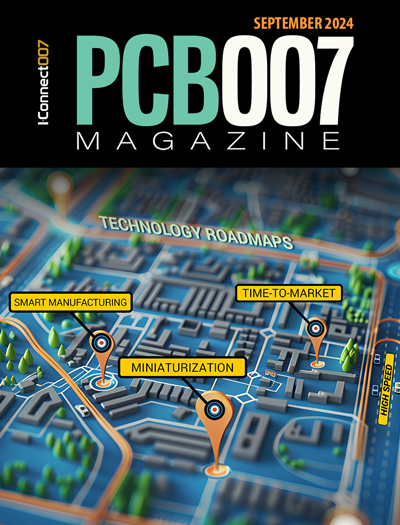
Technology Roadmaps
In this issue of PCB007 Magazine, we discuss technology roadmaps and what they mean for our businesses, providing context to the all-important question: What is my company’s technology roadmap?
- Articles
- Columns
Search Console
- Links
- Media kit
||| MENU - pcb007 Magazine
SIA Applauds House Passage of Tax Relief for American Families and Workers Act
February 1, 2024 | SIAEstimated reading time: Less than a minute
The Semiconductor Industry Association (SIA) released the following statement from SIA President and CEO John Neuffer commending House passage tonight of the Tax Relief for American Families and Workers Act. The legislation includes two provisions critical to the semiconductor industry: the restoration of immediate domestic R&D expensing and the United States-Taiwan Expedited Double-Tax Relief Act. The bill passed by a vote of 357-70.
“The Tax Relief for American Families and Workers Act would strengthen the U.S. semiconductor industry by promoting innovation and removing impediments to business with one of our top trading partners, Taiwan. The legislation restores immediate domestic R&D expensing and aims to resolve tax matters between the U.S. and Taiwan, two provisions critical to boosting the competitiveness of the U.S. semiconductor industry and reaching the full potential of the CHIPS and Science Act. We applaud the House for approving the bill with strong, bipartisan support and urge the Senate to swiftly follow suit.”
Suggested Items
Western Digital CEO David Goeckeler Elected Chair of Semiconductor Industry Association
11/22/2024 | SIAThe Semiconductor Industry Association (SIA) today announced Western Digital CEO David Goeckeler has been elected Chair of the SIA Board of Directors. SIA represents 99% of the U.S. semiconductor industry by revenue and nearly two-thirds of non-U.S. chip firms.
PCB Design Software Market Expected to Hit $9.2B by 2031
11/21/2024 | openPRThis report provides an overview of the PCB design software market, detailing key market drivers, challenges, technological advancements, regional dynamics, and future trends. With a projected compound annual growth rate (CAGR) of 13.4% from 2024 to 2031, the market is expected to grow from USD 3.9 billion in 2024 to USD 9.2 billion by 2031.
SIA Applauds CHIPS Award for Semiconductor Research Corporation’s SMART USA Institute
11/21/2024 | SIAThe Semiconductor Industry Association (SIA) released the following statement from SIA President and CEO John Neuffer commending the announcement that the U.S. Department of Commerce and the Semiconductor Research Corporation Manufacturing Consortium Corporation (SRC) are entering negotiations for the Commerce Department to provide SRC $285 million to establish and operate the CHIPS Manufacturing USA Institute for Digital Twins.
SIA Praises Finalization of CHIPS Investments for GlobalFoundries Manufacturing Projects
11/21/2024 | SIAThe Semiconductor Industry Association (SIA) released the following statement from SIA President and CEO John Neuffer applauding finalization of semiconductor manufacturing investments announced by the U.S. Department of Commerce and GlobalFoundries.
CHIPS for America Announces Up to $300M in Funding to Boost U.S. Semiconductor Packaging
11/21/2024 | U.S. Chamber of CommerceThe Biden-Harris Administration announced that the U.S. Department of Commerce (DOC) is entering negotiations to invest up to $300 million in advanced packaging research projects in Georgia, California, and Arizona to accelerate the development of cutting-edge technologies essential to the semiconductor industry.


